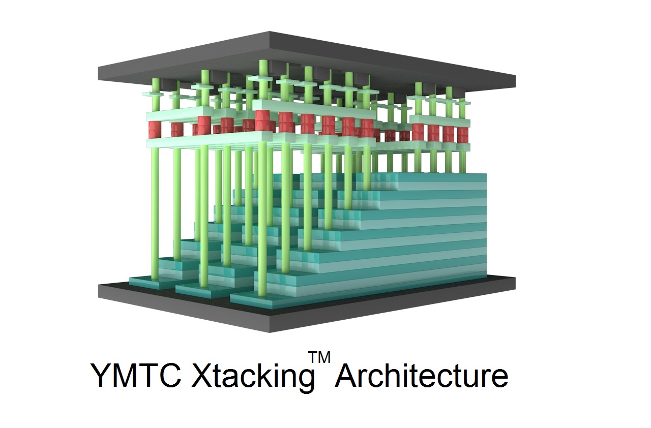
Yangtze Memory Technologies Co., Ltd (YMTC), a new player in the NAND industry,announced the market introduction of its ground-breaking technology - Xtacking, which will provide unprecedented NAND I/O performance, higher bit density and faster time-to-market.

With Xtacking, the periphery circuits which handle data I/O as well as memory cell operations are processed on a separate wafer using the logic technology node that enables the desired I/O speed and functions. Once the processing of the array wafer is completed, the two wafers are connected electrically through millions of metal VIAs (Vertical Interconnect Accesses) that are formed simultaneously across the whole wafer in one process step, using the innovative Xtacking technology, with limited increase in total cost.
“As monolithic die density increases with each successive generation of 3D NAND, it becomes much more challenging to maintain or improve performance for a given SSD capacity. Higher I/O speed and multi-plane operation will be necessary to achieve the required SSD performance going forward,” said Gregory Wong, Founder and Principal Analyst at Forward Insights, a renowned market intelligence firm in the field of NAND flash memories and solid-state storage.
“At present, the world’s highest 3D NAND I/O speed is targeting 1.4Gbps while the majority of the industry is offering NAND I/O at 1.0Gbps or below. With our Xtacking technology, it is possible for NAND I/O speed to reach up to 3.0Gbps, similar to I/O speed of DRAM DDR4. This is going to be a game changer in the NAND industry,” said Simon Yang, CEO at YMTC.
In the conventional 3D NAND architecture, the periphery circuits take up ~20-30% of the die area, lowering NAND bit density. As 3D NAND technology continues to progress to 128 layers and above, the periphery circuits will likely take up more than 50% of the total die area. With Xtacking, the periphery circuits are now above the array chip, enabling much higher NAND bit density than conventional 3D NAND.
Xtacking technology utilizes fully independent processing of the array and periphery, which offers a modularized, parallel approach to product development and manufacturing, reducing product development time by at least three months and shortening manufacturing cycle time by 20%, significantly accelerating 3D NAND time-to-market. This modular approach also opens possibilities for customized NAND flash solutions by the incorporation of innovative functionalities in the periphery.
YMTC has developed its 2nd generation 3D NAND utilizing this innovative Xtacking technology, targeting to go to mass production in 2019. With help from customers, industry partners and standard bodies, Xtacking ushers in a brand-new chapter in high-performance customized NAND solutions for smartphone, personal computing, data center and enterprise applications.
YMTC has successfully utilized this innovative Xtacking technology in its 2nd generation 3D NAND development, targeting to go to mass production in 2019. With help from customers, industry partners and standard bodies, Xtacking ushers in a brand-new chapter in high-performance customized NAND solutions for smartphone, personal computing, data center and enterprise applications. |